D-link DWL-900AP+ Hardware Overview
Hardware
- Mainboard
- GL2422AP-1T1-B0
- v1.1
- v1.2
- GL2422AP-1T1-B0
- PSU
- AIC1563CN
- Input voltage: Up to 30V
- Output voltage: 3.3Vdc
- Output current
- Peak: 2A
- Continuous: 1.5A
- AIC1563CN
- CPU
- Conexant CX82100-4X
- Core: ARM940T (ARM9TDMI)
- Max Clock Speed: 168MHz
- Unused peripherals
- USB1.1
- 1 x MII ethernet controllers
- Conexant CX82100-4X
- Flash
memory
- M29W800DB
- Capacity: 8Mbits = 1Mbyte
- 100,000 write/erase cycles
- M29W800DB
- SDRAM
- IC42S16400-7T
- Capacity: 64Mbits = 8Mbytes
- Max Clock Speed: 133MHz
- PLD
- EPM3032A
- CMOS EEPROM-based
- Interfaces with a hex inverter (AHC74)
- EPM3032A
- miniPCI
slot
- Probably miniPCI v1.0 compliant slot
- Wireless miniPCI: GL2422MP-MT2
- Ethernet
Physical Transceiver
- KS8721B
- Auto-negotiation
- 100BaseTX/FX
- 10BaseT
- Full/Half duplex
- KS8721B
- JTAG
connectors
- 14-pin (Embedded Ice compatible) for ARM9
- 10-pin for Altera PLD
- Serial
interface
- not installed
Below you can see the mainboard of DWL-900AP+ and the various ICs used on it. It must be at least a 3-layer PCB.
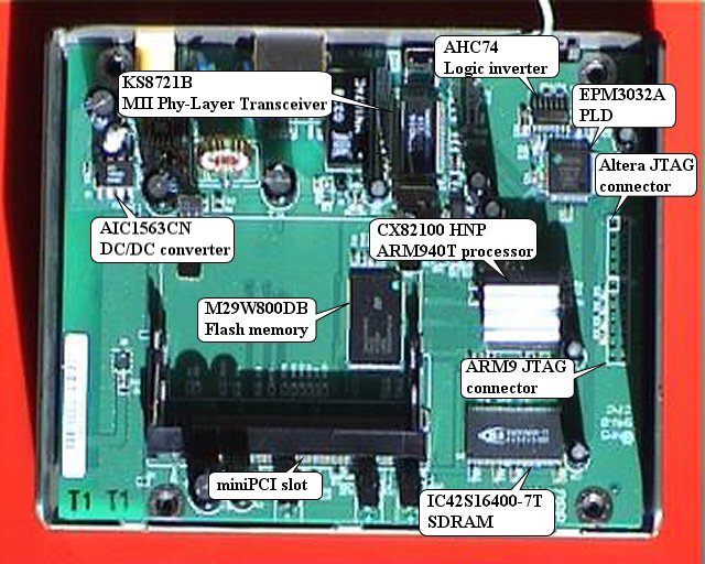
DWL-900AP+ Mainboard
The OEM vendor of this board is Global Sun. The OEM ID is GL2422AP-1T1-B10 and is printed on the mainboard together with a PCB version. I have come across two different PCB versions, v1.1 and v1.2. The latest is slightly different - some discrete capacitors have been replaced with SMD - but all the functions are identical.
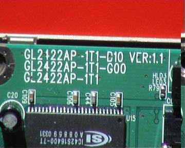
OEM ID: 2422AP-1T1-B10
The power supply section uses an AIC1563CN DC/DC converter to step the voltage from the power supply unit down to 3.3V. It can withstand input voltages up to 30V and can deliver 2A peak and 1.5A continuous current. According to the datasheet its efficiency is up to 90%. A POE system could be built by just injecting higher than the PSU voltage (but not above 10Volts) into UTP cable and letting this IC do all the job to bring it down. :-)
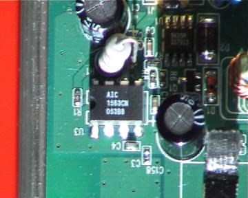
AIC1563CN DC/DC converter
The heart of the device is covered by a heatsink. It is the Conexant CX82100-4X Home Network Processor running at a maximum of 168 MHz. This processor is based on an ARM940T (ARM9TDMI) core, plus some peripherals. In fact not all of them are functional on this device. There is a USB 1.1 slave interface and a second ethernet controller which are not used by DWL-900AP+ nor they have any connectors to interface them. But they exist. ;-)
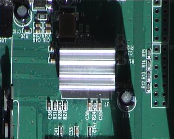
Under the heatsink is the CX82100-4X HNP
Flash ROM of the device is the M29W800DB from ST. Its capacity is 8Mbits which means 1MByte memory for an ARM processor. It can be programmed and erased under low voltages and is divided in blocks which can be programmed/erased individually. The guranteed lifetime of this IC is 100,000 write/erase cycles per block.
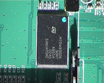
M29W800DB flash memory chip
The miniPCI slot seems to be a standard miniPCI v1.0 compliant slot. The wireless card put there is again by Global Sun GL2522MP-MT2 v1.1. A review for the wireless miniPCI card is here.
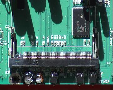
miniPCI slot
IC42S16400-7T is the RAM of the system. It is a SDRAM with a capacity of 64Mbits and a clock frequency up to 133MHz. 64Mbits for the ARM processor is 8MBytes of RAM.
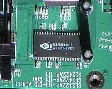
IC42S16400
A mysterious IC is the Altera EPM3032-A PLD. It is an EEPROM-based PLD with a Jtag interface. A hex inverter (AHC74) is also connected to it. I cannot imagine what could be the use for a PLD in 900AP+. If anyone has any idea why it might be there please let me know.
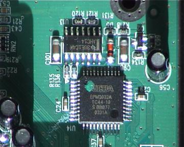
Altera EPM3032-A
The physical transceiver for the ethernet interface is the Kendin KS8721B. It provides media independent interface (MII) reception and transmission of data to CX82100 HNP. It also supports auto-negotiation and manual selection for 10/100Mbps speed and full/half duplex mode.
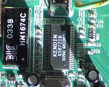
Kendin KS8721B
And finally the most interesting part. There are two Jtag connectors - one for ARM9 processor (J2) and one for Altera PLD (J5). The first is a standard 14-pin (embedded ICE) Jtag connector. I wonder if we could program the flash ROM through there with an embedded OS... ;-)
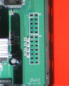
Jtag connectors
Unfortunately there isn't any UART installed in the device so as to watch how an embedded linux kernel loads. If anyone has information about flashing with an embedded OS or installing an UART please contact me.